- 您现在的位置:买卖IC网 > Sheet目录307 > ADE7758ARWZRL (Analog Devices Inc)IC ENERGY METERING 3PHASE 24SOIC
�� ��
��
��ADE7758�
�THEORY� OF� OPERATION�
�ANTIALIASING� FILTER�
�V2�
�Data� Sheet�
�This� filter� prevents� aliasing,� which� is� an� artifact� of� all� sampled�
�+500mV�
�VAP,� VBP,�
�OR� VCP�
�systems.� Input� signals� with� frequency� components� higher� than�
�half� the� ADC� sampling� rate� distort� the� sampled� signal� at� a� fre-�
�quency� below� half� the� sampling� rate.� This� happens� with� all� ADCs,�
�V� CM�
�SINGLE-ENDED� INPUT�
�±500mV� MAX� PEAK�
�COMMON-MODE�
�±25mV� MAX�
�V2�
�V� CM�
�V� N�
�regardless� of� the� architecture.� The� combination� of� the� high�
�sampling� rate� ∑-Δ� ADC� used� in� the� ADE7758� with� the� relatively�
�–500mV�
�AGND�
�low� bandwidth� of� the� energy� meter� allows� a� very� simple� low-�
�pass� filter� (LPF)� to� be� used� as� an� antialiasing� filter.� A� simple� RC�
�filter� (single� pole)� with� a� corner� frequency� of� 10� kHz� produces�
�an� attenuation� of� approximately� 40� dB� at� 833� kHz.� This� is� usually�
�sufficient� to� eliminate� the� effects� of� aliasing.�
�ANALOG� INPUTS�
�The� ADE7758� has� six� analog� inputs� divided� into� two� channels:�
�current� and� voltage.� The� current� channel� consists� of� three� pairs�
�of� fully� differential� voltage� inputs:� IAP� and� IAN,� IBP� and� IBN,�
�and� ICP� and� ICN.� These� fully� differential� voltage� input� pairs�
�have� a� maximum� differential� signal� of� ±0.5� V.� The� current�
�channel� has� a� programmable� gain� amplifier� (PGA)� with� possible�
�gain� selection� of� 1,� 2,� or� 4.� In� addition� to� the� PGA,� the� current�
�channels� also� have� a� full-scale� input� range� selection� for� the� ADC.�
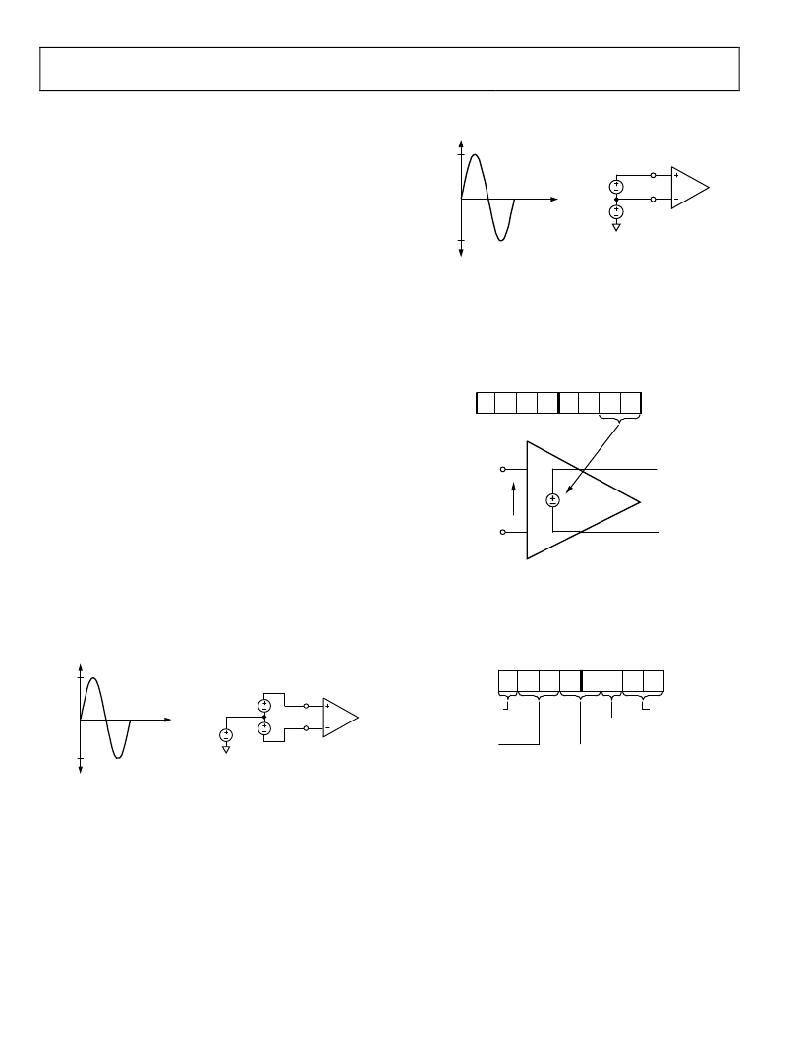
�Figure� 37.� Maximum� Signal� Levels,� Voltage� Channels,� Gain� =� 1�
�The� gain� selections� are� made� by� writing� to� the� gain� register.�
�Bit� 0� to� Bit� 1� select� the� gain� for� the� PGA� in� the� fully� differential�
�current� channel.� The� gain� selection� for� the� PGA� in� the� single-�
�ended� voltage� channel� is� made� via� Bit� 5� to� Bit� 6.� Figure� 38�
�shows� how� a� gain� selection� for� the� current� channel� is� made�
�using� the� gain� register.�
�GAIN[7:0]�
�GAIN� (K)�
�SELECTION�
�IAP,� IBP,� ICP�
�The� ADC� analog� input� range� selection� is� also� made� using� the�
�gain� register� (see� Figure� 38).� As� mentioned� previously,� the�
�maximum� differential� input� voltage� is� ±0.5� V.� However,� by�
�using� Bit� 3� and� Bit� 4� in� the� gain� register,� the� maximum� ADC�
�input� voltage� can� be� set� to� ±0.5� V,� ±0.25� V,� or� ±0.125� V� on� the�
�V� IN�
�IAN,� IBN,� ICN�
�K� � V� IN�
�current� channels.� This� is� achieved� by� adjusting� the� ADC� reference�
�(see� the� Reference� Circuit� section).�
�Figure� 36� shows� the� maximum� signal� levels� on� the� current�
�channel� inputs.� The� maximum� common-mode� signal� is�
�±25� mV,� as� shown� in� Figure� 37.�
�V� 1� +� V� 2�
�Figure� 38.� PGA� in� Current� Channel�
�Figure� 39� shows� how� the� gain� settings� in� PGA� 1� (current�
�channel)� and� PGA� 2� (voltage� channel)� are� selected� by� various�
�bits� in� the� gain� register.�
�GAIN� REGISTER� 1�
�CURRENT� AND� VOLTAGE� CHANNEL� PGA� CONTROL�
�7� 6� 5� 4� 3� 2� 1� 0�
�+500mV�
�IAP,� IBP,�
�0�
�0�
�0�
�0�
�0�
�0�
�0�
�0�
�ADDRESS:� 0x23�
�DIFFERENTIAL� INPUT�
�V� 1� +� V� 2� =� 500mV� MAX� PEAK�
�V� 1�
�OR� ICP�
�INTEGRATOR� ENABLE�
�PGA� 1� GAIN� SELECT�
�±25mV� MAX�
�01� =� ×2�
�V� CM�
�–500mV�
�COMMON-MODE� V� 2�
�V� CM� IAN,� IBN,�
�OR� ICN�
�Figure� 36.� Maximum� Signal� Levels,� Current� Channels,� Gain� =� 1�
�0� =� DISABLE�
�1� =� ENABLE�
�PGA� 2� GAIN� SELECT�
�00� =� ×1�
�01� =� ×2�
�10� =� ×4�
�00� =� ×1�
�RESERVED�
�10� =� ×4�
�CURRENT� INPUT� FULL-SCALE� SELECT�
�00� =� 0.5V�
�01� =� 0.25V�
�10� =� 0.125V�
�The� voltage� channel� has� three� single-ended� voltage� inputs:� VAP,�
�VBP,� and� VCP.� These� single-ended� voltage� inputs� have� a�
�maximum� input� voltage� of� ±0.5� V� with� respect� to� VN.� Both� the�
�1� REGISTER�
�CONTENTS� SHOW� POWER-ON� DEFAULTS�
�Figure� 39.� Analog� Gain� Register�
�current� and� voltage� channel� have� a� PGA� with� possible� gain�
�selections� of� 1,� 2,� or� 4.� The� same� gain� is� applied� to� all� the� inputs�
�of� each� channel.�
�Figure� 37� shows� the� maximum� signal� levels� on� the� voltage�
�Bit� 7� of� the� gain� register� is� used� to� enable� the� digital� integrator�
�in� the� current� signal� path.� Setting� this� bit� activates� the� digital�
�integrator� (see� the� DI/DT� Current� Sensor� and� Digital� Integrator�
�section).�
�channel� inputs.� The� maximum� common-mode� signal� is�
�±25� mV,� as� shown� in� Figure� 36.�
�Rev.� E� |� Page� 18� of� 72�
�发布紧急采购,3分钟左右您将得到回复。
相关PDF资料
ADE7761AARSZ-RL
IC ENERGY METERING 1PHASE 20SSOP
ADE7761BARSZ-RL
IC ENERGY METERING 1PHASE 20SSOP
ADE7768ARZ-RL
IC ENERGY METERING 1PHASE 16SOIC
ADE7769ARZ-RL
IC ENERGY METERING 1PHASE 16SOIC
ADM8843ACPZ-REEL7
IC LED DRVR WHITE BCKLGT 16LFCSP
ADP1653ACPZ-R7
IC LED DRVR PHOTO FLASH 16-LFCSP
ADP1712-EVALZ
BOARD EVALUATION ADP1712
ADP1720-EVALZ
BOARD EVAL FOR ADP1720-ADJ
相关代理商/技术参数
ADE7759
制造商:AD 制造商全称:Analog Devices 功能描述:Active Energy Metering IC with di/dt Sensor Interface
ADE7759ARS
功能描述:IC ENERGY METERING 1PHASE 20SSOP RoHS:否 类别:集成电路 (IC) >> PMIC - 能量测量 系列:- 产品培训模块:Lead (SnPb) Finish for COTS
Obsolescence Mitigation Program 标准包装:2,500 系列:*
ADE7759ARSRL
功能描述:IC ENERGY METERING 1PHASE 20SSOP RoHS:否 类别:集成电路 (IC) >> PMIC - 能量测量 系列:- 产品培训模块:Lead (SnPb) Finish for COTS
Obsolescence Mitigation Program 标准包装:2,500 系列:*
ADE7759ARSZ
功能描述:IC ENERGY METERING 1PHASE 20SSOP RoHS:是 类别:集成电路 (IC) >> PMIC - 能量测量 系列:- 产品培训模块:Lead (SnPb) Finish for COTS
Obsolescence Mitigation Program 标准包装:2,500 系列:*
ADE7759ARSZRL
功能描述:IC ENERGY METERING 1PHASE 20SSOP RoHS:是 类别:集成电路 (IC) >> PMIC - 能量测量 系列:- 产品培训模块:Lead (SnPb) Finish for COTS
Obsolescence Mitigation Program 标准包装:2,500 系列:*
ADE7760
制造商:AD 制造商全称:Analog Devices 功能描述:Energy Metering IC with On-Chip Fault Detection
ADE7760ARS
制造商:Analog Devices 功能描述:Energy Measurement 20-Pin SSOP 制造商:Analog Devices 功能描述:ENERGY METER IC W/ ONCHIP FAULT & OSCIL. - Rail/Tube
ADE7760ARSRL
制造商:Analog Devices 功能描述:Energy Measurement 20-Pin SSOP T/R 制造商:Analog Devices 功能描述:ENERGY METER IC W/ONCHIP FAULT & OSCIL. - Tape and Reel